- This topic is empty.
-
AuthorPosts
-
As modern electronics continue to demand more functionality in smaller footprints, multilayer PCB assembly has become the preferred foundation for advanced device design. Industries ranging from consumer tech and medical diagnostics to automotive control and aerospace navigation rely on multilayer boards to achieve exceptional performance, stability, and compactness. This article outlines the essential processes behind multilayer PCB assembly and how SprintPCB delivers seamless, end-to-end manufacturing support.
Understanding Multilayer PCB Assembly
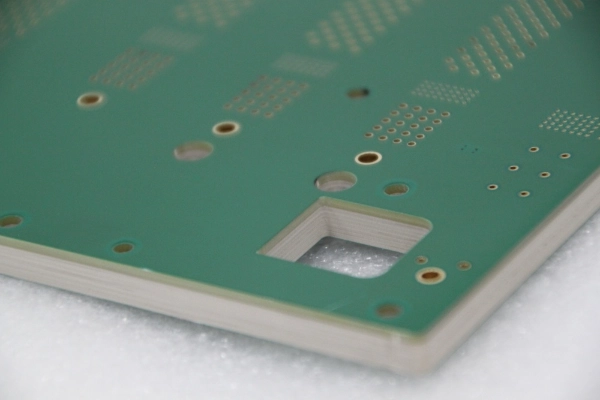
Multilayer PCB assembly involves building and assembling circuit boards constructed from three or more copper layers, bonded together with insulating materials under controlled heat and pressure. Vias—whether through-hole, blind, or buried—facilitate electrical communication between layers.
This layered structure enables engineers to integrate complex circuits without increasing board size. In high-speed, space-constrained applications such as smartphones, servers, and medical equipment, multilayer PCBs offer enhanced signal integrity, lower electromagnetic interference, and improved overall durability.
Essential Steps in Multilayer PCB Assembly
Producing a dependable multilayer board involves meticulous coordination across several critical stages. The accuracy of each step ultimately determines the board’s electrical performance and long-term reliability.
1. Multilayer PCB Fabrication
The process begins by laminating copper foils with dielectric substrates to create the required layer stack. Drilling is then carried out to form vias connecting different copper layers.
Even slight deviations during lamination or drilling can compromise alignment, leading to signal issues—making precision the cornerstone of quality multilayer PCB manufacturing.2. Solder Paste Printing
Solder paste is accurately deposited onto component pads using laser-cut stencils.
This ensures every pad receives the correct amount of paste, which is vital for preventing solder bridges, insufficient joints, and other assembly defects common in dense multilayer designs.3. Component Mounting (SMT & THT)
Automated SMT machines place components rapidly and precisely, including high-pin-count packages like BGAs.
For connectors or parts requiring higher mechanical strength, THT insertion is used. Combining SMT and THT allows multilayer boards to support both delicate microelectronics and rugged interface components.4. Reflow and Wave Soldering
Once components are mounted, soldering takes place:
-
Reflow soldering secures SMT devices
-
Wave or selective soldering is used for THT parts
Carefully controlled temperature profiles prevent common issues such as cold joints, solder voids, or thermal damage—especially important for multilayer PCBs with tightly packed components.
5. Inspection and Electrical Testing
To ensure performance under demanding conditions, the assembled boards undergo multiple inspection and testing procedures:
-
Automated Optical Inspection (AOI) for surface-level solder defects
-
X-ray inspection for verifying hidden BGA and QFN joints
-
In-Circuit Testing (ICT) to confirm electrical continuity and component values
-
Functional testing to validate real-world operation
These steps guarantee consistent quality before boards enter production or deployment.
SprintPCB: Complete Multilayer PCB Assembly Under One Roof
SprintPCB differentiates itself by offering a fully integrated manufacturing ecosystem. Instead of outsourcing, every phase—from bare board fabrication to final testing—is handled in-house, enabling faster lead times, tighter process control, and more reliable output.
SprintPCB’s one-stop capabilities include:
-
High-precision PCB fabrication for multilayer stacks
-
Laser-cut stencil production for accurate paste printing
-
Global component sourcing with cost and authenticity assurance
-
SMT, THT, BGA, and mixed-technology assembly
-
IC programming for mainstream microcontrollers and ICs
-
Comprehensive AOI, ICT, X-ray, and functional testing
-
Scalable production: prototypes to high-volume batches
-
End-to-end turnkey solutions covering manufacturing, sourcing, and assembly
This integrated model minimizes risks, improves communication, and ensures consistent quality across every multilayer PCB assembly project.
Conclusion
Multilayer PCB assembly is essential to the evolution of modern electronics. Its ability to deliver compact size, high performance, and strong reliability makes it the backbone of today’s most advanced products. Every step—from lamination and soldering to inspection—must be executed with precision to ensure optimal results. With its comprehensive in-house capabilities, SprintPCB offers a streamlined and dependable pathway from concept to finished product, making it an ideal partner for companies developing next-generation electronic systems.
http://www.sprintpcb.net
SprintPCB -
-
AuthorPosts